<- previous index next ->
Below is a schematic of a one clock per instruction computer.
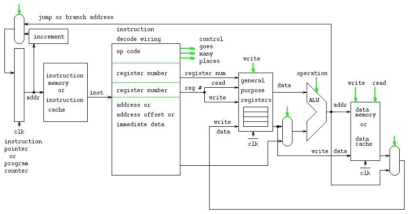 The operation for each instruction is:
The Instruction Pointer Register contains the address of the
next instruction to be executed.
The instruction address goes into the Instruction Memory or
Instruction Cache and the instruction comes out.
"inst" on the diagram.
The Instruction Decode has all the bytes of the instruction:
The instruction has bits for the operation code.
e.g. there is a different bit pattern for add, sub, etc.
Most instructions will reference one register. The register
number has enough bits to select one of the general registers.
Many instructions have a second register. (Not shown here,
on some computers there can be three registers.) The second
(or third) register may be the register number that receives
the result of the operation.
Many instructions have either a memory address for a operand or
a memory offset from a register or immediate data for use by
the operation. This data is passed into the ALU for use by
the operation, either for computing a result or computing
an address.
The general registers receive two register numbers and very
quickly output the data from those two registers.
The ALU receives two data values and control from the
Operation Code part of the instruction. The ALU computes
the value and outputs the value on the line labeled "addr".
This line goes three places: To the mux and possibly into
the Instruction Pointer if the operation is a jump or a branch.
To the Data Memory or Data Cache if the value is a computed
memory address. To the mux that may return the value to a register.
The Data Memory or Data Cache receives an address and write data.
Depending on the control signals "write" and "read":
The Data Memory reads the memory value and send it to the mux.
The Data Memory writes the "write date" into memory at
the memory location "addr".
The final mux may take a value just read from the Data Memory
or Data Cache and return that value to a register or
take the computed value from the ALU and return that value
to a register.
While the above signals are propagating, the Instruction Pointer
is updated by either incrementing by the number of bytes in the
instruction or from the jump or branch address.
This is one instruction, the clock transitions and the next instruction
is started.
The timing consideration that limits the speed of this design is
the long propagation from the new Instruction Pointer value until
the register is written. Notice that the register is written on
clock_bar and the Data Cache is written on clock_bar. Any real
computer must use instruction and data caches for this design
because RAM memory access is slower than logic on the CPU chip.
Another digital logic high level schematic of a CPU:
part1.ps
One reason we need computers?
view
go virtual
The operation for each instruction is:
The Instruction Pointer Register contains the address of the
next instruction to be executed.
The instruction address goes into the Instruction Memory or
Instruction Cache and the instruction comes out.
"inst" on the diagram.
The Instruction Decode has all the bytes of the instruction:
The instruction has bits for the operation code.
e.g. there is a different bit pattern for add, sub, etc.
Most instructions will reference one register. The register
number has enough bits to select one of the general registers.
Many instructions have a second register. (Not shown here,
on some computers there can be three registers.) The second
(or third) register may be the register number that receives
the result of the operation.
Many instructions have either a memory address for a operand or
a memory offset from a register or immediate data for use by
the operation. This data is passed into the ALU for use by
the operation, either for computing a result or computing
an address.
The general registers receive two register numbers and very
quickly output the data from those two registers.
The ALU receives two data values and control from the
Operation Code part of the instruction. The ALU computes
the value and outputs the value on the line labeled "addr".
This line goes three places: To the mux and possibly into
the Instruction Pointer if the operation is a jump or a branch.
To the Data Memory or Data Cache if the value is a computed
memory address. To the mux that may return the value to a register.
The Data Memory or Data Cache receives an address and write data.
Depending on the control signals "write" and "read":
The Data Memory reads the memory value and send it to the mux.
The Data Memory writes the "write date" into memory at
the memory location "addr".
The final mux may take a value just read from the Data Memory
or Data Cache and return that value to a register or
take the computed value from the ALU and return that value
to a register.
While the above signals are propagating, the Instruction Pointer
is updated by either incrementing by the number of bytes in the
instruction or from the jump or branch address.
This is one instruction, the clock transitions and the next instruction
is started.
The timing consideration that limits the speed of this design is
the long propagation from the new Instruction Pointer value until
the register is written. Notice that the register is written on
clock_bar and the Data Cache is written on clock_bar. Any real
computer must use instruction and data caches for this design
because RAM memory access is slower than logic on the CPU chip.
Another digital logic high level schematic of a CPU:
part1.ps
One reason we need computers?
view
go virtual
<- previous index next ->