<- previous index next ->
We now focus on sequential logic. Logic with storage and state.
The previous lectures were on combinational logic, gates.
In order to build very predictable large digital logic systems,
synchronous design is used. A synchronous system has a special
signal called a master clock. The clock signal continuously
has values 0101010101010 ... . This is usually just a square
wave generator at some frequency. A clock with frequency 1 GHz
has a period of 1 ns. Half of the period the clock is a logical 1
and the other half of the clock period the clock is a logical 0.
___ ___ ___
clk ___| |___| |___|
|< 1 ns>|
The VHDL code fragment to generate the clk signal is:
signal clk : std_logic := '0';
begin
clk <= not clk after 500 ps;
A synchronous system is designed with registers that input a
value on a raising clock edge, hold the signal until the next
raising clock edge. The designer must know the timing of
combinational logic because the signals must propagate through
the combinational logic in less than a clock time.
Combinational logic can not have loops or feedback.
Sequential logic is specifically designed to allow loops and
feedback. The design rule is that and loop or feedback must
include a storage element (register) that is clocked.
+------------------------------------+
| |
| +---------------+ +----------+ |
+->| combinational |-->| register |--+
| logic | | |
+---------------+ +----------+
^
| clock signal
A register may be many bits and each bit is built from a flip flop.
A flip flop is ideally either in a '1' state or a '0' state.
The most primitive flip flop is called a latch. A latch can be made
from two cross coupled nand gates. The latch is not easy to work
with in large circuits, thus JK flip flops and D flip flops are
typically used. In modern large scale integrated circuits, the
flip flops and thus the registers are designed at the device level.
A classical model of a JK flip flop is
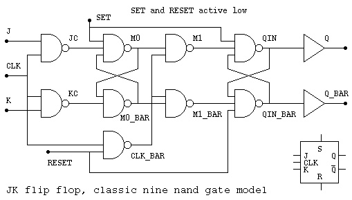 On the raising edge of the clock signal,
if J='1' the Q output is set to '1'
if K='1' the Q output is set to '0'
if both J and K are '1', the Q signal is inverted.
Note that Q_BAR is the complement of Q in the steady state.
There is a transient time when both could be '1' or both could be '0'.
The SET signal is normally '1' yet can be set to '0' for a short
time in order to force Q='1' (set the flip flop).
The RESET signal is normally '1' yet can be set to '0' for a short
time in order to force Q='0' (reset the flip flop or register to zero).
A slow counter, called a ripple counter, can be made from JK flip
flops using the following circuit:
On the raising edge of the clock signal,
if J='1' the Q output is set to '1'
if K='1' the Q output is set to '0'
if both J and K are '1', the Q signal is inverted.
Note that Q_BAR is the complement of Q in the steady state.
There is a transient time when both could be '1' or both could be '0'.
The SET signal is normally '1' yet can be set to '0' for a short
time in order to force Q='1' (set the flip flop).
The RESET signal is normally '1' yet can be set to '0' for a short
time in order to force Q='0' (reset the flip flop or register to zero).
A slow counter, called a ripple counter, can be made from JK flip
flops using the following circuit:
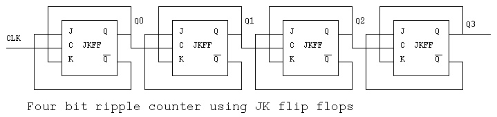 The VHDL source code for the entity JKFF, the JK flip flop,
and the four bit ripple counter is jkff_cntr.vhdl
The Cadence run file is jkff_cntr.run
The Cadence output file is jkff_cntr.out
ncsim: 04.10-s017: (c) Copyright 1995-2003 Cadence Design Systems, Inc.
ncsim> run 340 ns
q3, q2, q1, q0 q3_ q2_ q1_ q0_ clk
0 0 0 0 1 1 1 1 1 at 10 NS
0 0 0 1 1 1 1 0 1 at 30 NS
0 0 1 0 1 1 0 1 1 at 50 NS
0 0 1 1 1 1 0 0 1 at 70 NS
0 1 0 0 1 0 1 1 1 at 90 NS
0 1 0 1 1 0 1 0 1 at 110 NS
0 1 1 0 1 0 0 1 1 at 130 NS
0 1 1 1 1 0 0 0 1 at 150 NS
1 0 0 0 0 1 1 1 1 at 170 NS
1 0 0 1 0 1 1 0 1 at 190 NS
1 0 1 0 0 1 0 1 1 at 210 NS
1 0 1 1 0 1 0 0 1 at 230 NS
1 1 0 0 0 0 1 1 1 at 250 NS
1 1 0 1 0 0 1 0 1 at 270 NS
1 1 1 0 0 0 0 1 1 at 290 NS
1 1 1 1 0 0 0 0 1 at 310 NS
0 0 0 0 1 1 1 1 1 at 330 NS
________________________________________________________________
reset
_ _ _ _ _ _ _ _ _ _ _ _ _ _ _ _
clk | |_| |_| |_| |_| |_| |_| |_| |_| |_| |_| |_| |_| |_| |_| |_| |_
___ ___ ___ ___ ___ ___ ___ ___
q0 ___| |___| |___| |___| |___| |___| |___| |___| |
_______ _______ _______ _______
q1 _______| |_______| |_______| |_______| |
_______________ _______________
q2 _______________| |_______________| |
_______________________________
q3 _______________________________| |
Ran until 340 NS + 0
ncsim> exit
In many designs, only one input is needed and the resulting flip flop
is a D flip flop. A D flip flop needs 6 nand gates rather than the
9 nand gates needed by the JK flip flop. There is a proportional
reduction is devices when the flip flop is designed from basic
transistors.
The VHDL source code for the entity JKFF, the JK flip flop,
and the four bit ripple counter is jkff_cntr.vhdl
The Cadence run file is jkff_cntr.run
The Cadence output file is jkff_cntr.out
ncsim: 04.10-s017: (c) Copyright 1995-2003 Cadence Design Systems, Inc.
ncsim> run 340 ns
q3, q2, q1, q0 q3_ q2_ q1_ q0_ clk
0 0 0 0 1 1 1 1 1 at 10 NS
0 0 0 1 1 1 1 0 1 at 30 NS
0 0 1 0 1 1 0 1 1 at 50 NS
0 0 1 1 1 1 0 0 1 at 70 NS
0 1 0 0 1 0 1 1 1 at 90 NS
0 1 0 1 1 0 1 0 1 at 110 NS
0 1 1 0 1 0 0 1 1 at 130 NS
0 1 1 1 1 0 0 0 1 at 150 NS
1 0 0 0 0 1 1 1 1 at 170 NS
1 0 0 1 0 1 1 0 1 at 190 NS
1 0 1 0 0 1 0 1 1 at 210 NS
1 0 1 1 0 1 0 0 1 at 230 NS
1 1 0 0 0 0 1 1 1 at 250 NS
1 1 0 1 0 0 1 0 1 at 270 NS
1 1 1 0 0 0 0 1 1 at 290 NS
1 1 1 1 0 0 0 0 1 at 310 NS
0 0 0 0 1 1 1 1 1 at 330 NS
________________________________________________________________
reset
_ _ _ _ _ _ _ _ _ _ _ _ _ _ _ _
clk | |_| |_| |_| |_| |_| |_| |_| |_| |_| |_| |_| |_| |_| |_| |_| |_
___ ___ ___ ___ ___ ___ ___ ___
q0 ___| |___| |___| |___| |___| |___| |___| |___| |
_______ _______ _______ _______
q1 _______| |_______| |_______| |_______| |
_______________ _______________
q2 _______________| |_______________| |
_______________________________
q3 _______________________________| |
Ran until 340 NS + 0
ncsim> exit
In many designs, only one input is needed and the resulting flip flop
is a D flip flop. A D flip flop needs 6 nand gates rather than the
9 nand gates needed by the JK flip flop. There is a proportional
reduction is devices when the flip flop is designed from basic
transistors.
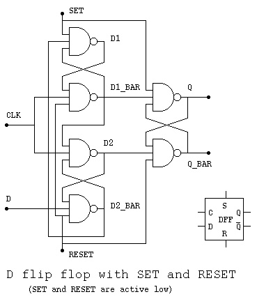 The VHDL source code for the entity DFF, the D flip flop,
and the four bit counter is dff_cntr.vhdl
The Cadence run file is dff_cntr.run
The Cadence output file is dff_cntr.out
The VHDL source code for the D flip flops:
dff.vhdl
Entity dff1 is five nand model
Entity dff2 is six nand model
The Cadence run file is dff.run
The Cadence output file is dff.out
Similar Verilog source code
dff.v
test_dff.v
test_dff_v.out
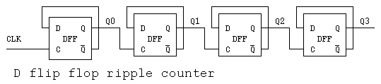
The D flip flop ripple counter
The VHDL source code for the entity DFF, the D flip flop,
and the four bit counter is dff_cntr.vhdl
The Cadence run file is dff_cntr.run
The Cadence output file is dff_cntr.out
The VHDL source code for the D flip flops:
dff.vhdl
Entity dff1 is five nand model
Entity dff2 is six nand model
The Cadence run file is dff.run
The Cadence output file is dff.out
Similar Verilog source code
dff.v
test_dff.v
test_dff_v.out
The D flip flop ripple counter
<- previous index next ->